Materials Center Leoben Forschung GmbH

Our Testing Laboratories & Technical Equipment

We bring cutting-edge technology together under one roof. We offer state-of-the-art testing laboratories with high-end systems and methods in every specific area of materials testing and materials analysis. They enable us to examine, characterize, and optimize materials on both the microscopic and macroscopic level. From the development of new materials to the improvement of existing production processes – our technical equipment helps you continually push the limits of what is possible.


Metallography & Light Microscopy

Mechanical Testing Laboratory

Physical / Chemical Laboratory

Electron Microscopy Laboratory

Microelectronics Testing Laboratory

Heat Treatment & Mechanical Workshop


A look inside our test labs

Materials testing under pressurised hydrogen influence
Metallographic section preparation
Mechanical testing laboratory – CT sample setup for fracture mechanics testing
Electron microscope for high-resolution imaging and chemical analysis
Inert gas heat treatment of small batches
Residual stress measuring system
CNC sample manufacture
Atomic Force Microscope - AFM

Our laboratories in detail

Mechanical testing laboratory

Mechanical Testing Laboratory

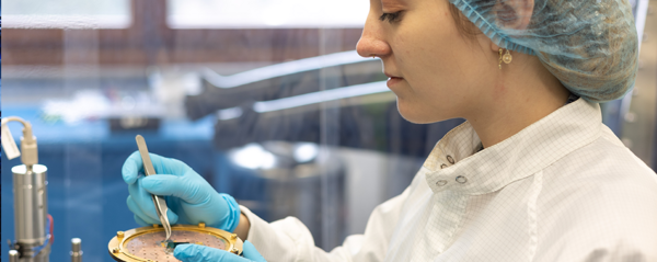
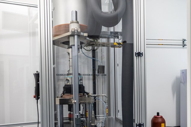
The mechanical testing laboratory specializes in determining the strength, hardness, and fatigue life of a wide variety of materials and components. Using high-precision tensile, compression, and bending test machines, hardness testers, and supporting measurement equipment, we deliver reliable results for design, quality assurance, and research.

  • Hardness testers (Emco Test DV30G5, Qness Q10A+).
  • Universal testing machines (Zwick Z250) up to 250 kN, optionally with high-temperature furnace up to 900 °C.
  • Hydropuls test systems (Instron 8802, 8803, 8854; Schenk PS100) with inductive heating, vacuum chamber, temperature ranges from -150 °C to 900 °C, and high-precision laser extensometers.
  • Resonance testing machines (Russenberger Testronic & Mikrotron-20) with high-temperature furnaces and temperature chambers.
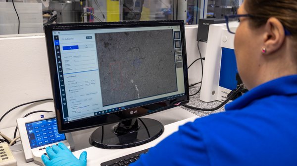
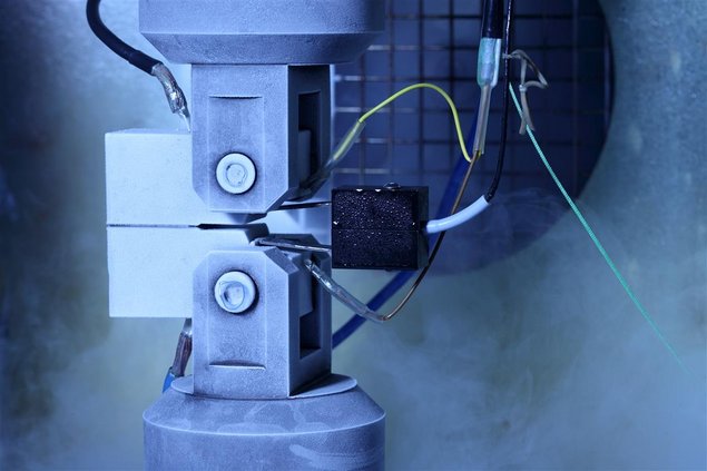
  • DCPD/ACPD measurement systems (Matelect + in-house design) for in-situ crack length measurements.
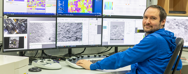
  • Optical 3D deformation measurement system (ARAMIS) for precise motion and shape analysis.

👉 Comprehensive materials and component testing – from static tests to dynamic high-load and high-temperature experiments.


Mechanical Workshop

Test sample manufacturing & mechanical workshop

Our in-house workshop provides the foundation for accurate testing: CNC milling and turning machines, precision saws, and automated preparation systems make it possible to manufacture customized specimens in all geometries. This ensures optimal preparation for all subsequent tests – fast, flexible, and precise.

  • CNC lathes and milling machines for precise specimen production in all geometries.
  • Band saws and rough/fine cutting machines for defined cuts.
  • Target preparation devices for ultra-precise specimen machining.
  • Waterjet cutting (cooperation partner) for complex contours and special shapes.

👉 Flexible and precise specimen manufacturing – the basis for high-quality materials analysis.

Microelectronics Laboratory

Microelectronics Laboratory

The microelectronics laboratory focuses on the analysis and reliability testing of electronic components and assemblies. Equipped with inspection and test systems combined with SEM/EDX analytics, we examine material quality, defects, and interconnect reliability – from the surface down to the nanostructure.

  • Computed tomography (Nanotom) for non-destructive 3D analysis.
  • Confocal UV Raman microscope (Witec alpha300R) for chemical and structural characterization.
  • Bond testers (SigmaCondor) and μDMA (RSA-G2) for interconnect and material reliability.
  • Temperature testing technology: climatic cycling chambers, shock chambers for extreme testing.
  • Electrical analysis: TF Analyzer 3000, TDTR PicoTR, PU/SMU/frequency generators.
  • Scanning probe microscope (Semilab) for nanoscale surface analysis.
  • Precision sample preparation with Leica TXP EM.

👉 High-tech for micro- and nanoelectronics – comprehensive, precise, and application-oriented.

Heat Treatment Technology Center

Heat Treatment Technology Center

Our heat treatment facility enables targeted adjustment and modification of material properties. With laboratory furnaces under protective gas or vacuum, tempering and hardening systems, and precise temperature control, we can generate defined material states and prepare them for further testing – controlled, reproducible, and fully documented.

  • Quenching dilatometer (Bähr DLI 805L) with inductive heating system and integrated gas cooling.
  • Vacuum furnace (Systherms) with high-pressure gas quenching up to 14 bar.
  • Protective gas furnaces (N₂/argon) up to 1200 °C, circulating air chamber furnaces up to 850 °C.
  • Induction hardening test stand (ITP) for practice-oriented hardening and tempering tests including water/gas quenching.
  • Laser flash apparatus (Netzsch LFA 427) for thermophysical properties (-60 °C to 1200 °C).
  • Push-rod dilatometer (Netzsch DIL 402 CD) for length change measurements (-150 °C to 1200 °C).

👉 Precise heat treatment and thermal analysis – from laboratory trials to industry-relevant applications.

Electron Microscopy Laboratory

Scanning Electron Microscopy Laboratory (SEM / High-Resolution SEM / FIB-SEM)

In the field of electron microscopy, our expertise lies in detailed surface and microstructure characterization down to the nanometer scale. With high-end FE-SEM and dual-beam systems, multi-detectors (SE, BSE, EBSD, EDX, SIMS, and more), and modular extensions such as nanoindenters, heating and cryo modules, or AFM, we enable analyses and in-situ experiments at the highest level. TEM foils and micro-samples are prepared directly in-house.

  • High-end SEM systems (Zeiss EVO MA25®, Gemini® 450, CrossBeam® 340/550 with FIB) for analyses down to the nanometer scale.
  • Versatile modules: tensile/compression/bending stages, nanoindenter, heating/cryogenic modules, AFM.
  • Multi-detectors & analytics: SE, BSE, STEM, EBSD/TKD, EDX/WDX, SIMS.
  • Precise sample preparation: TEM foils, atom probe tips, micro-samples, flat milling, coating.

👉 Everything from a single source – state-of-the-art electron microscopy for maximum level of detail.

Physical-Chemical Laboratory

Physical-Chemical Laboratory (XRD)

The physical-chemical laboratory offers state-of-the-art X-ray diffractometry (XRD) for the analysis of crystal structures, phases, and residual stresses. With high-resolution detectors, flexible measuring modes, and software methods such as Rietveld refinement or 3D-XRD, powders, thin films, and complex components can all be characterized with high precision.

  • Bruker D8 Discover with ultra-precise ATLAS goniometer, flexible anode materials and detectors, including high-temperature chamber HTK2000 (25–1400 °C).
  • Seifert Charon SXL for large-volume components, high-precision measurements with spot sizes down to 50 μm.
  • Mobile X-ray diffractometers (Stresstech Xstress 3000 G2/G3) for depth measurements, internal surfaces, and in-situ analyses.
  • Mobile X-ray fluorescence analyzer (Bruker S1 TurboLE) for rapid on-site material analysis.

👉 High-precision X-ray technology – stationary and mobile, from laboratory analysis to in-situ measurement.

Laboratory for Metallography and Light Microscopy

Laboratory for Metallography and Light Microscopy

The metallography laboratory is characterized by state-of-the-art equipment for the preparation and analysis of metallic materials, metal-ceramic composites, hard metals, and special materials. With precise cutting and CNC machining equipment, automated grinding and polishing lines, mounting and etching technology, as well as high-resolution light and stereo microscopy, we offer a complete process chain – from specimen production to detailed microstructural analysis. Supported by digital image analysis and 3D confocal microscopy, we obtain clear, reproducible results for research, development, and quality assurance.

  • Precise specimen production with CNC milling and turning machines as well as rough and fine cutting systems.
  • Mounting, grinding, and polishing technology – automated and manual, including electrochemical polishing and etching.
  • Top-level microscopy: light and stereo microscopy with digital 3D imaging, automated x-y stage for large areas.
  • Quantitative image analysis & profilometry with Nanofocus μsurf confocal microscope.
  • Advanced structural analysis in combination with scanning electron microscopes (SEM).

👉 State-of-the-art specimen preparation and microstructure analysis – for crystal-clear insights down to the finest details.