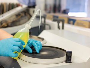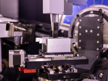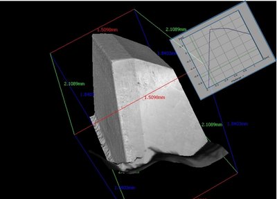

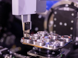
Metallography & Light Microscopic Microstructure Analysis
Characterization of the microstructure and microstructural composition of structural components and functional parts.
Our Focus Areas / Expertise
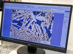
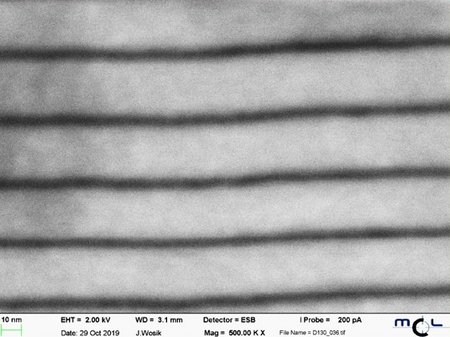
- Microstructure presentation and documentation
- Comprehensive range of etching techniques (chemical and electrochemical) for steels, non-ferrous metals, hard metals, etc.
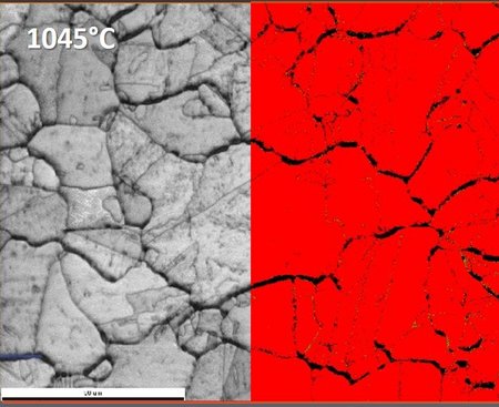
Evaluation according to a wide variety of standards
- Cleanliness assessment according to DIN 50602, ASTM E45,
DIN EN 10247 and ISO 4967 - Assessment of carbide banding and carbide networks according to SEP 1520
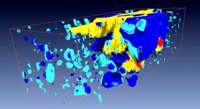
- Grain size determination according to DIN EN ISO 643 and
ASTM E112 - Surface decarburization according to DIN EN ISO 3887
- Cleanliness assessment according to DIN 50602, ASTM E45,