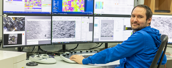
Scanning Electron Microscopy Laboratory (SEM / High-Resolution SEM / FIB-SEM)
In the field of electron microscopy, our expertise lies in detailed surface and microstructure characterization down to the nanometer scale. With high-end FE-SEM and dual-beam systems, multi-detectors (SE, BSE, EBSD, EDX, SIMS, and more), and modular extensions such as nanoindenters, heating and cryo modules, or AFM, we enable analyses and in-situ experiments at the highest level. TEM foils and micro-samples are prepared directly in-house.
- High-end SEM systems (Zeiss EVO MA25®, Gemini® 450, CrossBeam® 340/550 with FIB) for analyses down to the nanometer scale.
- Versatile modules: tensile/compression/bending stages, nanoindenter, heating/cryogenic modules, AFM.
- Multi-detectors & analytics: SE, BSE, STEM, EBSD/TKD, EDX/WDX, SIMS.
- Precise sample preparation: TEM foils, atom probe tips, micro-samples, flat milling, coating.
👉 Everything from a single source – state-of-the-art electron microscopy for maximum level of detail.