Materials Center Leoben Forschung GmbH

High-Resolution Electron Microscopy

  • High-resolution microstructural characterization with magnifications up to 1,000,000x.
  • Various electron and ion contrast modes, EBSD crystallographic information mapping
  • Measurement of crystal structure using EBSD from the centimetre scale down to structures as small as 20–30 nm
  • Determination of local chemical composition, elemental distributions, and particle analysis (EDX, WDX, XRF, FIB-SIMS (TOF))
  • Visualisation of the layer structure of multilayer coatings

In-situ Temperature Transformation Analysis

High-resolution documentation of transformation kinetics of individual phase fractions.

  • In-situ heating and cooling experiments in the scanning electron microscope
  • Temperature range: –180 °C to 1045 °C

Heating rates:

  • 180 °C to 400 °C: up to 20 °C/min
  • 250 °C to 1045 °C: up to 250 °C/min
  • Temperature-dependent residual stress measurements on coatings
  • Analysis with different detectors (including EBSD)

3D Microstructure and Contour Analysis

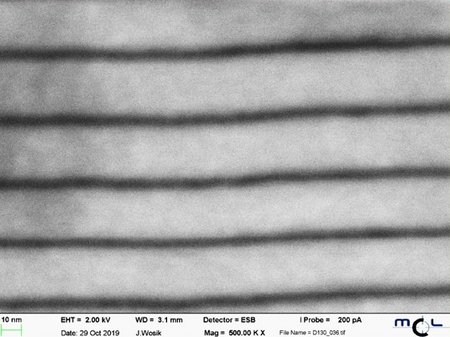
High-resolution 3D visualisation and measurement of contours and microstructural features.

Our Focus & Expertise

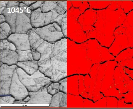
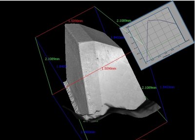
  • 3D topography of contours, damage, etc., including dimensional measurement from the millimetre down to the sub-micrometre range
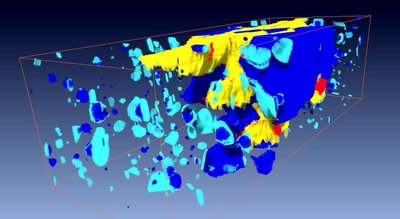
  • 3D tomography of microstructural constituents using the Slice & View method, including local chemistry and structure analysis
  • Various electron and ion contrast modes, EBSD crystallographic mapping, 3D elemental distributions, and depth profiles (EDX, EBSD, and FIB-SIMS (TOF))