Testing services / Methods / Competencies:
- Holistic evaluation of surface–boundary layer–substrate systems
- Combination of mechanical, microstructural and physical analysis methods
- Extensive experience with production-related issues in heat treatment, coating and post-processing, as well as specific topics such as thin and thick films in microelectronics (e.g. solder and bond layers)
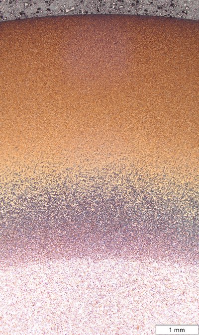
- Analysis of coatings, surface layers and near-surface material conditions (e.g. PVD/CVD layers, electroplated coatings, thermal spray coatings, chemical and mechanical surface treatments)
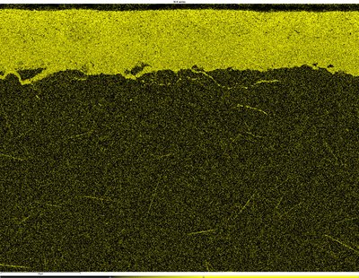
- Investigation of layer thickness, surface layer depth, microstructure, composition, hardness profiles, adhesive strength and defects using destructive and non-destructive testing methods
Specific technical features & information:
- Determination of surface layer and layer thicknesses in the µm to mm range
- Analysis of microstructure, phase distribution and hardness gradients
- Investigation of residual stresses resulting from heat or mechanical-thermal treatments
- Evaluation of interfaces, porosity, crack formation and adhesion problems
- Tests on flat-formed and complex components
Typical applications / practical examples
- Fault analysis on microelectronic assemblies, chips, substrates and packages
- Investigation of thermally damaged solder, bond or metal layers
- Analysis of crack formation and delamination after temperature change tests
- Testing of coated tools and functional components
- Evaluation of heat-treated functional components in mechanical and plant engineering
- Support with damage analysis, process approvals and product qualification